02203 Design of digital
systems (Fall 2023)
Below
you find a general description of the course, a description of the textbook and
other course material, and a tentative lecture plan.
1. General description of the course
About the course
The course requires some background
in: (1) digital electronics, including some experience using a hardware
description language e.g. VHDL, Verilog or similar, (2) elementary computer
architecture and (3) programming.
The course is an upper level
undergraduate course (for some students) or a graduate level course (for most
students). In more detail, the course can be characterized
as follows:
- A
first-level masters course for students enrolled
in one of the following of DTUs M.Sc.-programs: Computer Systems
Engineering, Electrical Engineering and Telecommunication.
- Next
level “up” for students enrolled in DTUs B.Sc. program in Electrical
Engineering (who follow a bottom-up approach (courses 02138+39)
- Next
level “down” students enrolled in DTUs B.Sc. program in Software
Technology (who follow a top down approach; course 02132)
- Elective
course for students B.Eng. program in Electrical Engineering (“Diplom E”)
Overall course
objectives:
- To
enable students to design large digital circuits in a systematic way and
to implement these in FPGA technology using typical CAD tools (currently:
VHDL and Xilinx
Vivado).
- To
enable students to analyze and optimize the
speed and area of a digital circuit.
Topics covered:
- Digital systems design: RTL-components and timing.
Pipelining. FSM+Data path (FSMD). Time
multiplexing.
- The VHDL language: Language
constructs. How to describe the intended circuitry in an efficient way.
- Design methodology:
Using VHDL, Top-down design flow, Simulation, Synthesis, FPGA technology, Tools: Xilinx Vivado.
- A small project during the
last half of the course. Some relatively small project that can be done within the semester. The design is taken all the way to a working FPGA implementation.
Project (you
pick one, A or B)
A: A min-heap circuit for dynamic pruning in AI accelerator
·
Used for dynamic pruning in neural networks (reduces
power and computational complexity)
·
Find the largest M elements in a stream of N elements
(M<<N)
·
Tree with M elements (so far):
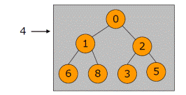
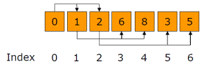
1: Build heap (first M elements)
6, 3, 0, 1, 8, 2, 5,
Ripple up
2: Maintain heap
Ripple down
·
Stored in an array (very efficient)
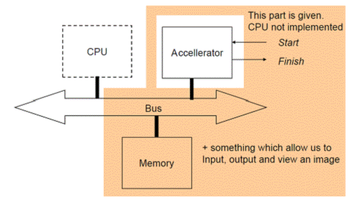
B: A co-processor (hardware accelerator) for
image processing.
Exam
- Written 2-hour exam and assessment of reports (GCD Lab &
Project).
The mark is given based on an overall assessment of reports and exam.
The course is
taught by: Professor
Jens Sparsø
2. Course material
·
Textbook: Pong P. Chu, “RTL hardware design using
VHDL”. Wiley. The book is sold by Polyteknisk
bookstore, and it is available as an E-book for on-line reading and downloading
through the DTU-library (login via DTU Inside).
- FPGA board
for lab exercises and design project.
Digilent Nexys4DDR board
with a XILINX Artix 7 FPGA.
- Supplementary
material
- Lecture
notes.
- On-line
resources from XILINX.
- Labs
and tutorials.
- Paper
and pencil problems.
3. More information about the textbook
|
|
From the back
cover … The skills and guidance needed to master RTL
hardware design. This book teaches readers how to
systematically design efficient, portable, and scalable Register
Transfer Level (RTL) digital circuits using the VHDL hardware description
language and synthesis software. Focusing on the module-level design, which
is composed of functional units, routing circuit, and storage, the book
illustrates the relationship between the VHDL constructs and the underlying
hardware components, and shows how to develop codes that faithfully reflect
the module-level design and can be synthesized into efficient gate-level
implementation. |

Several unique features distinguish the book:
·
Coding style that shows a clear relationship between
VHDL constructs and hardware components
·
Conceptual diagrams that illustrate the realization of
VHDL codes
·
Emphasis on the code reuse
·
Practical examples that demonstrate and reinforce
design concepts, procedures, and techniques
·
Two chapters on realizing sequential algorithms in
hardware
·
Two chapters on scalable and parameterized designs and
coding
·
One chapter covering the synchronization and interface
between multiple clock domains
Although the focus of the book is RTL synthesis, it
also examines the synthesis task from the perspective of the overall
development process. Readers learn good design practices and guidelines to
ensure that an RTL design can accommodate future simulation, verification, and
testing needs, and can be easily incorporated into a larger system or reused. Discussion is independent of technology and can be
applied to both ASIC and FPGA devices.
With a balanced presentation of fundamentals and
practical examples, this is an excellent textbook for upper-level undergraduate
or graduate courses in advanced digital logic. Engineers who need to make
effective use of today's synthesis software and FPGA devices should
also refer to this book
4. Tentative lecture plan (Fall 2023)
Version 1: July 5, 2023
Note: This
is a working document. Changes are likely to occur. Check for updates.
|
|
Lectures covering:
·
CAD
tools: Xilinx Vivado ·
Technology:
Nexys4DDR with Artix7 FPGA |
Labs / Problems |
|
L1 31/8 |
Course introduction, RT-Level design and
VHDL intro. Reading: Chu ch. 1, (8.1-8.2), slides. Papers on
hardware accelerators and dark silicon
Simulation
and synthesis using Xilinx Vivado ·
Introduction of the GCD lab o Just the problem and key idea of the lab, but no VHDL. |
Installing Xilinx Vivado on your laptop. Lab 0: VHDL and Xilinx Vivado brush up. Lab1:
GCD |
|
L2 7/9 |
VHDL 1: Introduction and
fundamentals. Reading: Chu ch.
2.1-2.2.5, 3.1-3.6, 4.1-4.6, 5, 6.1-6.4
and 6.6
Comb. Logic: Concurrent signal assignments
and/or process(all) with
sequential statements Registers: process(clk,reset)
o
Xilinx Vivado (Synthesis, placement, routing). o
|
Lab1: GCD |
|
L3 14/9 |
VHDL 2: Designing
FSMD-style circuits (the basics) Reading: Chu ch. 8.1-8.4.3,
8.9-8.10, 10.1-10.2, 10.5 ·
Introduction of FSMD
architecture (the concept). ·
FSM recap. State graphs.
Mealy/Moore. ASM charts. ·
Two-process VHDL template
/ REG-process and CL a set of concurrent signal assignments. |
Lab 1: GCD |
|
L4 21/9 |
VHDL 3 Systematic design of FSMD-style
circuits. Reading: Chu ch. 11. ·
RTL methodology: principle
and practice |
Lab 1. GCD Demo to TA |
|
L5 28/9 |
VHDL 4: Combinatorial and sequential
circuit design practice. Reading: Reading: Chu ch. 7.1-7.3.4,
7.5.2, 7.5.4, 7.6 Optimizing
the synthesized implementation by proper VHDL coding. ·
Presentation of Lab.2 Min-heap
or Edge detector |
Lab
1. GCD Demo to TA (last chance) Lab
2. Get started GCD report due 1/10 |
|
L6 5/10 |
Clocking, clock skew, and clock
distribution. Reading: Chu ch.
8.1-8.2, 8.6, 16.1-16.5, slides, problem. Papers on
clocking and reset
·
( Synchronization of input
signals ) |
Paper and pencil problems Lab
2. Work on project/Lab.2 |
|
L7 12/10 |
Memories and register files. Reading: Chu
9.3, Slides, XILINX-material
·
Initializing RAM’s as part
of the configuration |
Lab
2. Work on project/Lab.2 |
|
Autumn
break |
||
|
L8 26/10 |
Arithmetic circuits. Reading: Book chapter on arithmetic circuits (B&Wch5.pdf)
+ Slides
·
FPGA: Support for arithmetic
circuits (carry chains and hardwired 18bx18b multipliers) ·
How to write VHDL in order
to efficiently instantiate |
Lab
2. Work on project/Lab.2 |
|
L9 2/11 |
Student group presentations: Overall design and status/plan. Hard time limit: 5 min + 2 min for questions. No more than 4
slides allowed. |
Lab 2. Work on project/Lab.2 |
|
L10 9/11 |
Pipelining Reading: Chu. 9.4-9.5, PerformanceMeasuresMITchapter.pdf slides,
problems ·
Throughput and Latency ·
Data dependency graphs ·
How to systematically
pipeline (ex.: bubble-sort, adder …) ·
When pipelining is not possible
(recursion bottleneck) ·
How to write VHDL … |
Paper
and pencil problems. Lab
2. Work on project/Lab.2 |
|
L11 16/11 |
Interconnecting IP-cores: Reading: Slides, notes.
·
Packet switched on-chip interconnection networks. |
Lab
2. Work on project/Lab.2 |
|
L12 23/11 |
Problem solving + Research talk ·
8:15-9:00: Problem solving in class. W&H problem 8.4 , … ·
9:10-10:00: Computing without clocks / neural networks / Company
presentation / or … |
Lab 2. Demonstrate
your working design to TA. |
|
L13 30/11 |
Course evaluation and course wrap up. +
Problem solving |
3/12 Project report due. |